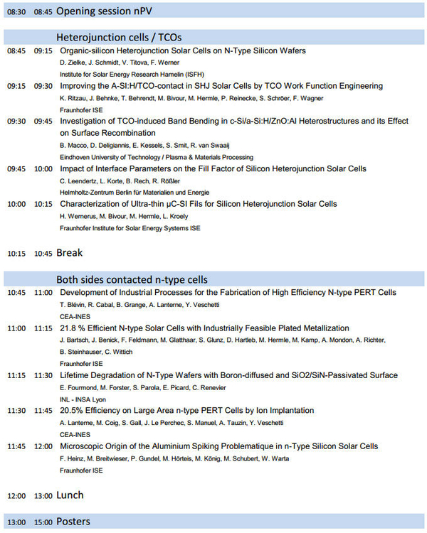
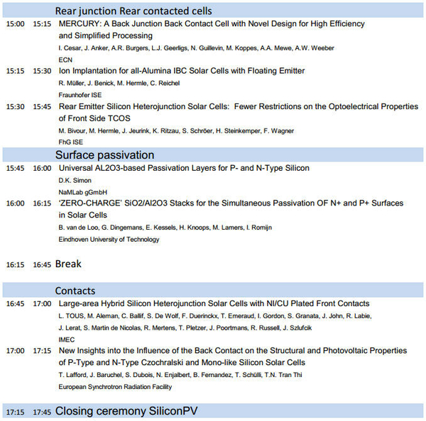
A Distributed Electrical Model for Interdigitated Back Contact Silicon Solar Cells
D. Giaffreda, University of Bologna |
Impact of Quantum Confinement Effect on Roles of Amorphous Silicon Layers in Heterojunction Solar Cells
T. Kamioka, Toyota Technological Institute | |
2D-Modeling of Metallization Losses in P+ Emitters Assuming SCHOTTKY Barriers and Tunneling
L.J. Koduvelikulathu, International Solar Energy Research Center Konstanz | |
Conceptual Comparison between Standard Si Solar Cells and Back Contacted Cells
A. Ali, Government College University Faisalabad | |
Accouting for Side Effects in Silicon Heterojunction Simulation
R. Varache, CEA, LITEN, LCP | |
Rear Contact Pattern Optimization Based on 3D Simulations for IBC Solar Cells with Point-Like Doped Contacts
D. Carrio, Universitat Politecnica de Catalunya | |
Analysis of the Impact of Doping Levels on Performance of Back Contact - Back Junction Solar Cells
P. Procel, DIMES. Università della Calabria | |
Exclusively Thermal Donor-doped CZ Wafers for High Efficiency Heterojunction Solar Cells
F. JAY, CEA-Liten National Institute of Solar Energy | |
Iron-boron Pair Kinetic in Compensated N-Type Silicon
C. Möller, CiS Forschungsinstitut für Mikrosensorik und Photovoltaik GmbH | |
UMG N-Type CZ-Silicon: Influencing Factors of the Light Induced Degradation and its Suitability for PV Production
J. Broisch, Fraunhofer Institute for Solar Energy Systems ISE | |
Optimized Texturization and Passivation of Silicon Heterojunction Solar Cells
B. Stegemann, HTW Berlin - University of Applied Sciences | |
Chemical Treatment for Improved Surface Passivation of Textured Silicon Heterojunction Solar Cells
D. Deligiannis, TU Delft | |
Boron Implanted, Laser Annealed P+ Emitter for N-Type Interdigitated Back-Contact Solar Cells
X. Yang, Research School of Engineering, The Australian National University | |
Boron Emitters from Doped PECVD Layers for n-type Crystalline Solar Cells with LCO
J. Engelhardt, Universität Konstanz | |
Recombination Losses Analysis in Rear Emittter Silicon Heterojunction Solar Cells
R. Varache, CEA, LITEN, LCP | |
Influence of Interfacial ITO Doping on the Fill Factor of n- and p-type SHJ Solar Cells
M. Bivour, FhG ISE | |
Etch-back of p+ Structures for Selective Boron Emitters in N-type c-Si Solar Cells
Y. Schiele, University of Konstanz | |
SHJ Solar Cells Based on a-Si:H/Al¬2O3/ZnO Stacks: Experimental Results and a New Quantitative Analysis of the Band Structure
S. Smit, Eindhoven University of Technology | |
Single-layer ITO vs ITO/ZNO:AL Layer Stacks in A-SI:H/C-SI Solar Cells: A Comparison
R. Rößler, Helmholtz-Zentrum Berlin | |
N-Type c-Si Solar Cells based on Laser Processed Dielectric
I. Martin, Departament d'Enginyeria Electònica. Universitat Politècnica de Catalunya | |
Selective Emitter Formation on N-type Silicon Wafers by Laser-chemical Processes
D. Linaschke, Fraunhofer IWS Dresden | |
Potential Advantage of an Industrially Processed Boron Emitter Compared to a Phosphorus Emitter
Y. Komatsu, ECN Solar Energy | |
Hydrogen Plasma Treatments of Amorphous/Crystalline Silicon Heterojunctions
M. Mews, Helmholtz-Zentrum Berlin | |
Passivation Properties of Subnanometer Thin Interfacial Silicon Oxide Films
W. Lu, Helmholtz Zentrum Berlin | |
DC Sputtered ZNO:AL as Alternative TCO in Silicon Heterojunction Solar Cells
K. von Maydell, EWE Forschungszentrum für Energietechnologie e. V. - NEXT ENERGY | |
Progress in Sputtering of Hydrogenated Amorphous Silicon for Silicon Solar Cells
X. Zhang, Australian National University | |
Exploration of Metastability of a-Si:H/c-Si Surface Passivation
R. Vasudevan, Delft University of Technology | |
Black Silicon in Interdigitated Back-contacted Solar Cells
P. Repo, Aalto University | |
Neutron and X-ray Reflectometry Investigations of Amorphous Silicon-based Surface Passivation Layers
E.S. Marstein, Institute for Energy Technology | |
Thermal, Structural and Electrical Study of the Effect of Annealing on the Passivation by A-Si of N-type Crystalline(100) Silicon Surfaces
H. Meddeb, Imec | |
Dielectric Passivation Schemes for High Efficiency N-type C-SI Solar Cells
M. Lamers, ECN Solar Energy | |
MF-Sputtered AZO for A-SI SHJ Solar Cells
J. Jeurink, Fraunhofer ISE | |
IBC-HJ Solar Cells with Electroplated Copper Contacts
Y. Ryabchikov, Lyon Institute of Nanotechnologies (INL, INSA de Lyon) | |
Improvement on Industrial N-type Bifacial Solar Cell with >20.6% Efficiency
H. Chang, Motech | |
Hard-mask Patterning of Hydrogenated Amorphous Silicon Layers for High Open-Circuit Voltage Back-contacted Silicon Heterojunction Solar Cells
B. Paviet-Salomon, École polytechnique fédérale de Lausanne (EPFL), Photovoltaics and Thin Film Electronics Laboratory | |
Wafer-thickness Dependence of Double-side Contacted Rear Junction N-type Solar Cells
T. Ballmann, Hanwha Q CELLS GmbH | |
Bifacial N-Type Silicon Solar Cells Fabricated by Co-diffusion
P. Rothhardt, Fraunhofer ISE | |
Laser Doped Screen Printed Back Contact Solar Cells Exceeding 21% Efficiency
M. Dahlinger, institute for photovoltaics | |
Adhesive Modification for Excellent Module-level a-Si:H Passivation of Wafers Bonded to Glass
S.N. Granata, IMEC / KU Leuven | |
Analyses of Potential-induced Degradation at Interdigitated Back Contact Solar Cells
V. Naumann, Fraunhofer Center for Silicon Photovoltaics CSP | |
| | |